Low Drop Voltage Regulator
TLE 4274
Features
•
•
•
•
•
•
•
•
•
•
Output voltage 5 V, 8.5 V or 10 V
Output voltage tolerance ≤ ±4%
Current capability 400 mA
Low-drop voltage
Very low current consumption
Short-circuit proof
Reverse polarity proof
Suitable for use in automotive electronics
Green Product (RoHS compliant) version of TLE 4274
AEC qualified
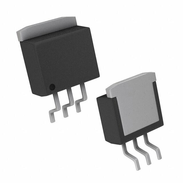
P-TO220-3-1
PG-TO220-3-1
^
Functional Description
P-TO252-3-11
The TLE 4274 is a low drop voltage regulator available in
a TO220, TO252 and TO263 package. The IC regulates
an input voltage up to 40 V to VQrated = 5.0 V (V50), 8.5 V
(V85) and 10 V (V10). The maximum output current is
400 mA. The IC is short-circuit proof and incorporates
temperature protection that disables the IC at
overtemperature. A 3.3 V and 2.5 V version is also
available. For information about the low output voltage
types please refer to the data sheet TLE 4274 / 3.3 V;
2.5 V.
PG-TO252-3-11
P-TO263-3-1
PG-TO263-3-1
Type
Package
TLE 4274 V10
PG-TO220-3-1 (RoHS compliant)
TLE 4274 V50
PG-TO220-3-1 (RoHS compliant)
TLE 4274 V85
PG-TO220-3-1 (RoHS compliant)
TLE 4274 DV50
PG-TO252-3-11 (RoHS compliant)
TLE 4274 GV10
PG-TO263-3-1 (RoHS compliant)
TLE 4274 GV50
PG-TO263-3-1 (RoHS compliant)
TLE 4274 GV85
PG-TO263-3-1 (RoHS compliant)
Data Sheet
1
Rev. 1.7, 2011-01-20
�TLE 4274
Dimensioning Information on External Components
The input capacitor CI is necessary for compensating line influences. Using a resistor of
approx. 1 Ω in series with CI, the oscillating of input inductivity and input capacitance can
be damped. The output capacitor CQ is necessary for the stability of the regulation circuit.
Stability is guaranteed at values CQ ≥ 22 μF and an ESR of ≤ 3 Ω within the operating
temperature range.
Circuit Description
The control amplifier compares a reference voltage to a voltage that is proportional to the
output voltage and drives the base of the series transistor via a buffer. Saturation control
as a function of the load current prevents any oversaturation of the power element. The
IC also includes a number of internal circuits for protection against:
•
•
•
Overload
Overtemperature
Reverse polarity
Data Sheet
2
Rev. 1.7, 2011-01-20
�TLE 4274
PG-TO220-3-1
GND
PG-TO252-3-11
PG-TO263-3-1
GND
GND
1
2
3
1
GND
I
2
3
Q
PG-TO252-3-11.vsd
1
2
I
3
GND
Q
PG-TO263-3-1.vsd
I
Q
GND
PG-TO220-3-1.vsd
Figure 1
Pin Configuration (top view)
Table 1
Pin Definitions and Functions
Pin No.
Symbol
Function
1
I
Input; block to ground directly at the IC with a ceramic capacitor.
2
GND
Ground
3
Q
Output; block to ground with a ≥ 22 μF capacitor, ESR ≤ 3 Ω.
TAB
-
TAB; connect to heatsink and GND to improve thermal
performance
Data Sheet
3
Rev. 1.7, 2011-01-20
�TLE 4274
Saturation
Control and
Protection
Circuit
Temperature
Sensor
Ι
1
3
Control
Amplifier
Q
Buffer
Bandgap
Reference
2
GND
AEB01959
Figure 2
Data Sheet
Block Diagram
4
Rev. 1.7, 2011-01-20
�TLE 4274
Table 2
Absolute Maximum Ratings
Tj = -40 to 150 °C
Parameter
Symbol
Limit Values
Unit
Test Condition
45
V
–
–
–
Internally limited
-1.0
40
V
–
–
–
–
Internally limited
IGND
–
100
mA
–
Tj
Tstg
–
150
°C
–
-50
150
°C
–
Min.
Max.
VI
II
-42
–
VQ
IQ
Input
Voltage
Current
Output
Voltage
Current
Ground
Current
Temperature
Junction temperature
Storage temperature
Note: Maximum ratings are absolute ratings; exceeding any one of these values may
cause irreversible damage to the integrated circuit.
Table 3
Operating Range
Parameter
Symbol
Limit Values
Unit
Remarks
Min.
Max.
Input voltage; V50, DV50, VI
GV50
5.5
40
V
–
VI
VI
Tj
9.0
40
V
–
10.5
40
V
–
-40
150
°C
–
Rthja
Rthja
Rthja
Rthjc
–
65
K/W
TO2201)
–
78
K/W
TO2521)
–
52
K/W
TO2631)
–
4
K/W
–
Input voltage, V85, GV85
Input voltage, V10, GV10
Junction temperature
Thermal Resistance
Junction ambient
Junction ambient
Junction ambient
Junction case
1) Worst case; regarding peak temperature, zero airflow mounted on PCB 80 × 80 × 1.5 mm3, 300 mm2 heat sink
area.
Data Sheet
5
Rev. 1.7, 2011-01-20
�TLE 4274
Table 4
Characteristics
VI = 13.5 V; -40 °C < Tj < 150 °C (unless otherwise specified)
Parameter
Symbol
Limit Values
Min.
Typ.
Max.
Unit
Measuring Conditions
Output voltage
V50-Version
VQ
4.8
5
5.2
V
5 mA < IQ < 400 mA
6 V < VI < 28 V
Output voltage
V50-Version
VQ
4.8
5
5.2
V
5 mA < IQ < 200 mA
6 V < VI < 40 V
Output voltage
V85-Version
VQ
8.16
8.5
8.84
V
5 mA < IQ < 400 mA
9.5 V < VI < 28 V
Output voltage
V85-Version
VQ
8.16
8.5
8.84
V
5 mA < IQ < 200 mA
9.5 V < VI < 40 V
Output voltage
V10-Version
VQ
9.6
10
10.4
V
5 mA < IQ < 400 mA
11 V < VI < 28 V
Output voltage
V10-Version
VQ
9.6
10
10.4
V
5 mA < IQ < 200 mA
11 V < VI < 40 V
Output current
limitation1)
IQ
400
600
–
mA
–
Current
consumption;
Iq = II - IQ
Iq
–
100
220
μA
IQ = 1 mA
Current
consumption;
Iq = II - IQ
Iq
Iq
–
–
8
20
15
30
mA
mA
IQ = 250 mA
IQ = 400 mA
Drop voltage1)
Vdr
–
250
500
mV
Load regulation
ΔVQ
–
20
50
mV
Line regulation
ΔVQ
–
10
25
mV
Power supply
ripple rejection
PSRR
–
60
–
dB
IQ = 250 mA
Vdr = VI - VQ
IQ = 5 mA to 400 mA
ΔVl = 12 V to 32 V
IQ = 5 mA
fr = 100 Hz;
Vr = 0.5 Vpp
–
0.5
–
mV/K –
Temperature
dVQ/dT
output voltage drift
1) Measured when the output voltage VQ has dropped 100 mV from the nominal value obtained at VI = 13.5 V.
Data Sheet
6
Rev. 1.7, 2011-01-20
�TLE 4274
ΙΙ
Input
1
3
CΙ
100 nF
100 μ F
ΙQ
Output
CQ
22 μF
TLE 4274
VΙ
VQ
2
RL
AES01960
Figure 3
Measuring Circuit
3
1
Input
Output
TLE 4274
CΙ
CQ
2
AES01961
Figure 4
Data Sheet
Application Circuit
7
Rev. 1.7, 2011-01-20
�TLE 4274
Typical Performance Characteristics (V50, V85 and V10)
Drop Voltage Vdr versus
Output Current IQ
Vdr
Output Current IQ versus
Input Voltage VI
AED01962
600
mV
IQ
AED01963
800
mA
500
600
400
T j = 25 ˚C
VQ = 0 V
T j = 125 ˚C
400
300
200
200
T j = 25 ˚C
100
0
0
100
200
0
300 mA 400
0
10
20
30
40 V 50
IQ
VI
Current Consumption Iq versus
Output Current IQ (high load)
Current Consumption Iq versus
Output Current IQ (low load)
AED02267
60
Iq mA
Iq mA
50
0.5
40
0.4
T j = 25 ˚C
VI = 13.5 V
30
AED02268
0.6
T j = 25 ˚C
VI = 13.5 V
0.3
20
0.2
10
0.1
0
0
100
200 300 400
mA
0
600
Data Sheet
0
10
20
30
40
mA
60
IQ
IQ
8
Rev. 1.7, 2011-01-20
�TLE 4274
Typical Performance Characteristics (V50)
Output Voltage VQ versus
Junction Temperature Tj
Current Consumption Iq versus
Input Voltage VI
AED01966
5.2
AED02269
30
VQ V
Ιq
mA
5.1
20
VI = 13.5 V
T j = 25 C
R L = 20 Ω
5.0
10
4.9
4.8
-40
0
40
80
0
120 ˚C 160
0
10
20
30
Tj
Output Voltage VQ versus
Input Voltage VI
Input Current II versus
Input Voltage VI
AED01968
6
VQ
V
AED01977
3.5
mA
II
3.0
VQ
5
50
V
VΙ
2.5
4
2.0
VI = VQ
1.5
3
T j = 25 ˚C
R L = 20 Ω
T j = 25 ˚C
6.8kΩ
R L = 8.2
kΩ
1.0
2
0.5
1
0
0
0
2
4
6
-2
-50
8 V 10
Data Sheet
-25
0
25
V
50
VI
VI
9
Rev. 1.7, 2011-01-20
�TLE 4274
Typical Performance Characteristics for V85
Output Voltage VQ versus
Junction Temperature Tj
Current Consumption Iq versus
Input Voltage VI
AED01970
8.8
VQ
AED02270
30
V
8.7
Ιq
8.6
mA
20
VI = 13.5 V
T j = 25 C
R L = 20 Ω
8.5
8.4
10
8.3
8.2
-40
0
40
80
0
120 ˚C 160
0
10
20
30
Tj
Output Voltage VQ versus
Input Voltage VI
Input Current II versus
Input Voltage VI
AED01972
12
VQ
50
V
VΙ
AED03051
3.5
mA
II
3.0
V
10
VQ
2.5
8
2.0
VΙ =VQ
1.5
6
T j = 25 C
R L = 34 Ω
T j = 25 ˚C
R L = 12 kΩ
1.0
4
0.5
2
0
0
Data Sheet
0
4
8
12
-2
-50
16 V 20
VΙ
-25
0
25
V
50
VI
10
Rev. 1.7, 2011-01-20
�TLE 4274
Typical Performance Characteristics for V10
Output Voltage VQ versus
Junction Temperature Tj
Current Consumption Iq versus
Input Voltage VI
AED01974
10.3
AED02270
30
VQ V
Ιq
10.2
mA
20
10.1
VI = 13.5 V
T j = 25 C
R L = 20 Ω
10.0
10
9.9
9.8
9.7
-40
0
40
80
0
120 ˚C 160
0
10
20
30
Tj
Output Voltage VQ versus
Input Voltage VI
Input Current II versus
Input Voltage VI
AED01976
12
VQ
V
AED03048
3.5
mA
II
3.0
VQ
10
50
V
VΙ
2.5
8
2.0
VI = VQ
1.5
6
T j = 25 ˚C
R L = 34 Ω
T j = 25 ˚C
R L = 15 kΩ
1.0
4
0.5
2
0
0
0
4
8
12
-2
-50
16 V 20
Data Sheet
-25
0
25
V
50
VI
VI
11
Rev. 1.7, 2011-01-20
�TLE 4274
Package Outlines
10 ±0.2
A
9.9 ±0.2
B
2.8 ±0.2
4.4
1.27±0.1
0.05
C
0...0.15
13.5 ±0.5
4.55 ±0.2
2.4
9.25 ±0.2
1)
0...0.3
12.95
17±0.3
15.65 ±0.3
8.5 1)
3.7 -0.15
0.5 ±0.1
3x
0.75 ±0.1
2.4
1.05
2x 2.54
1)
0.25
M
A B C
Typical
All metal surfaces tin plated, except area of cut.
Metal surface min. x=7.25, y=12.3
GPT09361
Figure 5
PG-TO220-3-1 (Plastic Transistor Single Outline)
Green Product (RoHS-Compliant)
To meet the world-wide customer requirements for environmentally friendly products
and to be compliant with government regulations the device is available as a green
product. Green products are RoHS-Compliant (i.e Pb-free finish on leads and suitable
for Pb-free soldering according to IPC/JEDEC J-STD-020).
You can find all of our packages, sorts of packing and others in our
Infineon Internet Page “Products”: http://www.infineon.com/products.
Dimensions in mm
SMD = Surface Mounted Device
Data Sheet
12
Rev. 1.7, 2011-01-20
�TLE 4274
6.5 +0.15
-0.05
A
2.3 +0.05
-0.10
B
(5)
0.51 MIN.
0.15 MAX.
per side
0.5 +0.08
-0.04
0.9 +0.20
-0.01
0...0.15
0.8 ±0.15
(4.24) 1 ±0.1
9.98 ±0.5
6.22 -0.2
5.4 ±0.1
3x
0.75 ±0.1
0.5 +0.08
-0.04
2.28
4.57
0.1 B
0.25
M
A B
All metal surfaces tin plated,
except area of cut.
GPT09277
Figure 6
PG-TO252-3-11 (Plastic Transistor Single Outline)
Green Product (RoHS-Compliant)
To meet the world-wide customer requirements for environmentally friendly products
and to be compliant with government regulations the device is available as a green
product. Green products are RoHS-Compliant (i.e Pb-free finish on leads and suitable
for Pb-free soldering according to IPC/JEDEC J-STD-020).
You can find all of our packages, sorts of packing and others in our
Infineon Internet Page “Products”: http://www.infineon.com/products.
Dimensions in mm
SMD = Surface Mounted Device
Data Sheet
13
Rev. 1.7, 2011-01-20
�TLE 4274
4.4
10 ±0.2
1.27 ±0.1
B
0.1
A
8.5 1)
0.05
2.4
2.7 ±0.3
4.7 ±0.5
7.55 1)
(15)
9.25 ±0.2
1 ±0.3
0...0.3
0...0.15
0.75 ±0.1
0.5 ±0.1
1.05
8 ˚ MAX.
2.54
5.08
1)
0.25
M
A B
0.1 B
Typical
All metal surfaces: tin plated, except area of cut.
Metal surface min. x=7.25, y=6.9
GPT09362
Figure 7
PG-TO263-3-1 (Plastic Transistor Single Outline)
Green Product (RoHS-Compliant)
To meet the world-wide customer requirements for environmentally friendly products
and to be compliant with government regulations the device is available as a green
product. Green products are RoHS-Compliant (i.e Pb-free finish on leads and suitable
for Pb-free soldering according to IPC/JEDEC J-STD-020).
You can find all of our packages, sorts of packing and others in our
Infineon Internet Page “Products”: http://www.infineon.com/products.
Dimensions in mm
SMD = Surface Mounted Device
Data Sheet
14
Rev. 1.7, 2011-01-20
�TLE 4274
TLE 4274
Revision History:
2011-01-20
Previous Version:
1.5
Rev. 1.7
Page
Subjects (major changes since last revision)
general
Updated Infineon logo
#1
Added “AEC” and “Green” logo
#1
Added “Green Product” and “AEC qualified” to the feature list
#1
Updated Package Names to “PG-xxx”
general
Removed leadframe variant “P-TO-252-1”
#12, #13, #14
Added “Green Product” remark
#16
Disclaimer Update
#17
Updated Package Outlines (added TAB potential)
Data Sheet
15
Rev. 1.7, 2011-01-20
�Edition 2011-01-20
Published by
Infineon Technologies AG
81726 München, Germany
© Infineon Technologies AG 2007.
All Rights Reserved.
Legal Disclaimer
The information given in this document shall in no event be regarded as a guarantee of conditions or
characteristics (“Beschaffenheitsgarantie”). With respect to any examples or hints given herein, any typical values
stated herein and/or any information regarding the application of the device, Infineon Technologies hereby
disclaims any and all warranties and liabilities of any kind, including without limitation warranties of
non-infringement of intellectual property rights of any third party.
Information
For further information on technology, delivery terms and conditions and prices please contact your nearest
Infineon Technologies Office (www.infineon.com).
Warnings
Due to technical requirements components may contain dangerous substances. For information on the types in
question please contact your nearest Infineon Technologies Office.
Infineon Technologies Components may only be used in life-support devices or systems with the express written
approval of Infineon Technologies, if a failure of such components can reasonably be expected to cause the failure
of that life-support device or system, or to affect the safety or effectiveness of that device or system. Life support
devices or systems are intended to be implanted in the human body, or to support and/or maintain and sustain
and/or protect human life. If they fail, it is reasonable to assume that the health of the user or other persons may
be endangered.
�


 工商网监
湘ICP备2023018690号
工商网监
湘ICP备2023018690号
